


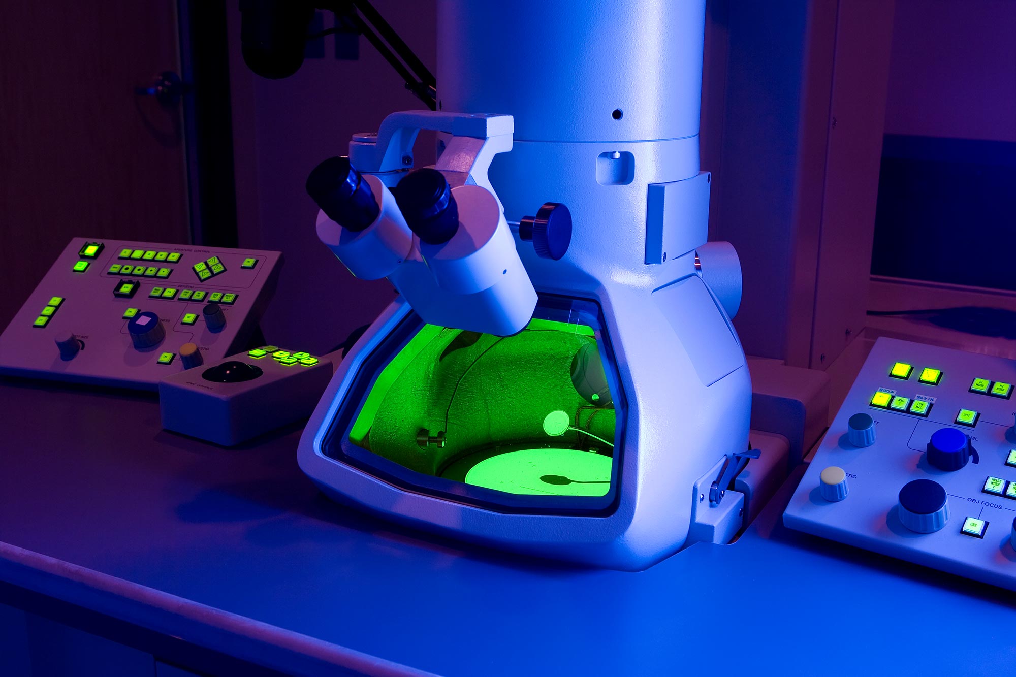
A Scanning Electron Microscope gives subtleties surface data by following an example in a raster design with an electron beam. These focal points are tubes, enveloped by a loop and alluded to as solenoids. The process starts with an electron weapon producing light emission electrons down the segment and onto a progression of electromagnetic lenses. The curls are acclimated to centre the occurrence electron pillar onto the example; these changes cause vacillations in the voltage, expanding/diminishing the speed at which the electrons interact with the example surface. Controlled through PC, the sem scanning electron microscope administrator can change the bar to control amplification to decide the surface region to be examined.
SEMs have an assortment of utilizations in various logical and industry-related fields, mainly where portrayals of solid materials are beneficial. In expansion to geological, morphological, and compositional data, a Scanning Electron Microscope can recognize and investigate surface cracks, give data in microstructures, analyze surface pollutions, uncover spatial varieties in compound creations, give subjective synthetic examinations and distinguish glasslike structures. Scanning electron microscope uses can be an entire exploration apparatus in fields like life science, science, gemology, clinical and scientific science, metallurgy. In expansion, SEMs have down-to-earth mechanical and innovative applications like semiconductor assessment, creating minuscule items, and gathering microprocessors for PCs.
Benefits of Scanning Electron Microscopy:
Here are a few advantages of utilizing sems electron microscope with EDS for material portrayal and failure examination.
Resolution Goal.
This test gives computerized picture goals as low as 15 nanometers, giving information describing microstructures like a break, consumption, grains, and grain limits.
Discernible norm for amplification.
Since all imaging is aligned to a detectable norm, it’s not difficult to apply investigation—such as covering thicknesses, grain size judgments, and molecule estimating—to saved pictures.
Synthetic investigation.
Microscope repair near me with EDS gives essential subjective investigation, standardless quantitative examination, x-beamline sweeps, and planning. This information can be utilized to analyze item abandons, recognize the natural structure of unfamiliar materials, evaluate the thickness of coatings, and decide grain and molecule size.
Examining electronic microscopy administrations give both high-goal typographical imaging just as subjective and quantitative substance investigation—benefits that are important to enterprises like general assembling, microelectronics, clinical gadgets, food preparing, innovative work, protection, and case support.
Let us look at the disadvantages of a Scanning Electron Microscope start with the size and cost:
- SEMs are costly, enormous and should be housed in a space liberated from any conceivable electric, attractive or vibration obstruction.
- Support includes keeping a consistent voltage, flows to electromagnetic curls and course of cool water.
- Special preparation is needed to work a sems electron microscope just as get ready examples.
- The planning of tests can bring about antiques. The adverse consequence can be limited with educated, experienced scientists who can distinguish antiquities from genuine information just as arrangement ability. There is no total method to dispense with or determine every single likely ancient rarity.
- Likewise, SEMs are restricted to solid and inorganic examples adequately, with little to fit inside the vacuum chamber that can deal with moderate vacuum pressure.
- At last, SEMs convey a slight danger of radiation openness related to the electrons that disperse from underneath the example surface.
The sample chamber is intended to avoid any electrical and attractive impedance, which ought to kill the opportunity of radiation getting away from the room. Even though the danger is negligible, sems electron microscope administrators and analysts are encouraged to notice wellbeing safety measures.
The distance that the natural eye can separate two sections in noticeable light is 0.2mm split. Anyway, this can be expanded using a focal point. This distance is known as the settling force of the focal point, which can amplify the distance many occasions over. A light magnifying lens has a settling staff of about 1000x, as it is restricted by the frequency of the light just as the quality and number of focal points utilized. Be that as it may, electron magnifying lenses give a more limited frequency, making a superior goal.
The spatial goal is subject to the size of the electron spot. Not at all like customary picture framing cameras (film or CCD cluster), SEM utilizes an electron pillar to quickly look over an example test to yield a picture. The goal of sems electron microscope is typically around 10 nanometres (nm).
The greatest goal for a filtering electron magnifying lens picture relies upon components, for example, the communication volume of the shaft and the electron spot size. SEMs can accomplish a high goal of under 1 nanometre (nm), even though they can’t give nuclear goals. Most current SEMS provide a purpose of 1-20 nm, while more modest work area renditions offer a plan of 20 nm or more.
The scanning electron microscope price is between 50,000 to 70,000 USD. The prices vary according to different countries.


